Guide to Experiment 3a: Transistor characterization
Métodos da Físcia Experimental I: (F540 2s2020)
JupyterBook: Gustavo Wiederhecker, Varlei Rodrigues
Contributions: Daniel Ugarte, Antônio Riul Junior, Varlei Rodrigues
#-----------------------------
#Pacote para manipular vetores e matrizes
import numpy as np
import os
import pandas as pd
#-----------------------------
#Pacotes para lidar com unidades
from astropy import units as un
from astropy import constants as cte
#-----------------------------
#pacote para gráficos
import matplotlib.pyplot as plt
import matplotlib
#Comandos opcionais para formatar gráfico
font = {'family' : 'Arial',
        'weight' : 'normal',
        'size'   : 12}
lines = {'linewidth' : 3.0}
figure = {'figsize' : [6.0, 6/1.6]}
matplotlib.rc('font', **font)
matplotlib.rc('lines', **lines)
matplotlib.rc('figure', **figure)
#-----------------------------
from myst_nb import glue
#pacote para desenhar circuitos
import SchemDraw as schem
import SchemDraw.elements as e
d = schem.Drawing(unit=2.5) # unit=2.5 determina o tamanho dos componentes
# %config InlineBackend.figure_format = 'svg'
In this experiment, the basic properties of a bipolar junctio transistor will be explored.
The name transistor (a combination of transfer + resistor)originates from this device capabiblity of transferring electric signals. It is an active device that amplifies the voltage or current of an input signal, therefore, it is necessary to use a power supply. The transistor is a sandwich of two pn junctions, facing each other, forming a sequence of \( npn \) or \( pnp \) junctions. Each of these parts is called the collector, base and emitter, and the information to be transferred and / or used as a control signal is applied to the base of the transistor.
To fully appreciate this device, it is desirable that you read an introductory text on the semiconductors properties and circuit treatment of transistors (Sections 4.1 to 4.3 in [1]).
Goals
Measure the characteristic curve of a bipolar junction transistor (BJT).
Measure the value of the current gain \( (\beta) \) of the BJT transistor.
Items to include in your lab report
From the experimental data, reconstruct the transistor collector curves (\(I_C(V_{CE})\)). You must generate the graphs, based on the data provided in Downloadable dataset.
Try to add the different traces to a single figure, instead of adding multiple repetitive plots to your report. Consider distinct line colors for each trace.
Be carefull to properly convert the voltage measurements into currents using the appropriate values for the resistors.
Include a graph of \(I_C(I_B)\) and determine the transistor gain.
Make sure to include the linear fitting you used to determine \(\beta\)
Provide hyperlinks to your TinkerCAD simulation and upload your QUCS file.
Characteristic curves (I-V curve)
presents characteristic curves for the bipolar junction transistor BD 135, being similar for other junction transistors. For each current value of the base there is a current in the collector, for which the equation below is satisfied:
In general, for (22) to be valid, if (\(V_{CE}\)) is higher than the \(V_{BE}\) , which is required to polarize the transistor into the active region. Play around with the background theory notebook ( Background: Solving Kirchhoof’s law for transistors using load lines) to get an insight into the the transistor behavior. An example of the IV curves generated at this notebook are shown in fig:transistor_gif:
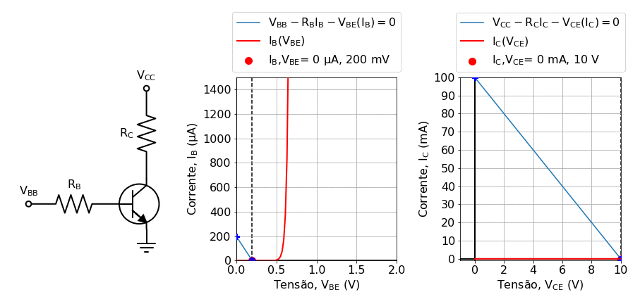
Fig. 21 Solving the transistor using the load line method for varying values of the base current. In this animation, generated in the notebook Background: Solving Kirchhoof’s law for transistors using load lines, the base voltage \(V_BB\) was varied in the range \(0.2 V\leq V_B\leq 1.2 V\).
Characteristics curves are often presented in transistor datasheets, such as the example in Fig. 29
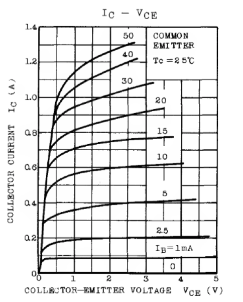
Fig. 22 Example datasheet from manufacturer showing transistor gain characterization
Transistor gain \(\beta\)
The gain of a transistor depends on its construction, current range and the frequency of operation of the circuit assembly. For the transistor BD 135, the characteristic curves as a function of the current \( I_B \) are illustrated in Fig. 31
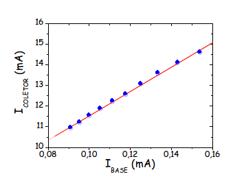
Fig. 23 Example dateset of transistor gain characterization
An approximate value of the \( (\beta) \) gain can be obtained on a linear graph of \( I_C \) as a function of \( I_B \), the gain being given by the slope of the line, as in the example of Fig. 31.
Measuring characterisitic curves
The characteristic curve of a transistor is the graph of \( I_C \) for \( V_ {CE} \). The proposed assembly for this measure is illustrated in the figure below. Note that the assembly is formed by a voltage divider (resistors \( R2 \) and \( R3 \)) that feeds the base of the transistor through the resistor \( R1 \), imposing a fixed \( (approximately) \) current of \( I_B \) at the base. After the transistor is polarized, the current in the collector will be given by the golden rule: \( I_ {collector} = \beta \times I_ {base} \).
To obtain the value of \( I_B \), it is necessary to measure the potential drop in the resistance of the base \( (R1) \). The potential on the transistor, between the collector and the emitter \( (V_{CE}) \), is measured directly with a voltmeter or with the oscilloscope.
Only the \( I_C \) measure is missing. Since the power supply is fixed at \( 15 V \), from the measurement of \( V_ {CE} \) and the resistance value of decades it is possible to calculate the current in the collector, \( I_C \). Therefore, it is enough to vary the resistance of decades to obtain each curve. Try to obtain a larger number of points in the region where the variation of \( V_ {CE} \) is more abrupt (lower values of voltage \( V_ {CE} \)). 3 \( I_C \) curves must be measured by \( V_ {CE} \), with \( R_1 \) = 10 k \( \Omega \), 15 k \( \Omega \) and 18 k \( \Omega \).
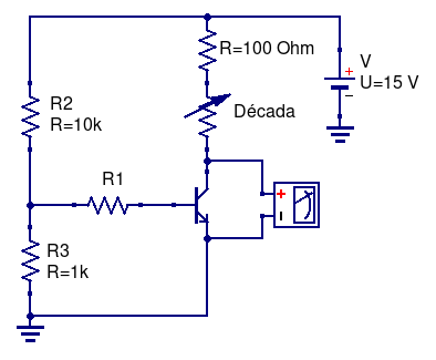
Fig. 24 Circuit schematic used in the transistor characterization
Measuring transistor Gain
The gain of the \( (\beta) \) transistor can be obtained simply by the ratio between the current in the collector and the current in the emitter, as previously shown. In a variation of the previous assembly, we can measure the gain of the transistor. We will use the a linear voltage ramp to vary the base voltage and, consequently, the current at the base of the transistor.
The current \( I_C \) is measured through the resistance \( RC \), while \( I_B \) is measured against the resistance \(R_B\). By controlling either the base voltage (\(V_{BB}\)), or the base resistace \(R_B\), it is possible to control \( I_B \).
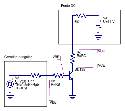
Fig. 25 Circuit schematic used in the transistor gain characterization. The internal resistance of the base voltage source is 50 Ohms.
Videos of the experiments
You must login with you @m.unicamp.br account to view these videos!
Characteristic curves
This first video illustrate the experimental procedure and data acquisition associated with the characteristic curves.
Transistor gain
This second video illustrate the experimental procedure and data acquisition associated with the transistor gain.
#Loading dataset with "tab" as separator
path='dados'
filename = 'dados_Vce_Vcc_15p5.csv'
filepath = os.path.join(path,filename)
df1 = pd.read_csv(filepath) #DataFrame
glue("df_pandas_ic_vce", df1.head())
#---
filename = 'dados_Ic_vs_Ib_Vbb_Vcc_15p5V.csv'
filepath = os.path.join(path,filename)
df2 = pd.read_csv(filepath) #DataFrame
glue("df_pandas_beta", df2.head())
| Rc(Ohm) | Vce_rb_10k(V) | Vce_rb_12k(V)k | Vce_rb_15k(V) | Vce_rb_20k(V) | |
|---|---|---|---|---|---|
| 0 | 100 | 13.86 | 14.10 | 14.29 | 14.43 |
| 1 | 200 | 12.82 | 13.22 | 13.61 | 13.89 |
| 2 | 300 | 11.75 | 12.40 | 12.87 | 13.32 |
| 3 | 400 | 10.71 | 11.57 | 12.20 | 12.81 |
| 4 | 500 | 9.70 | 10.70 | 11.54 | 12.28 |
| tempo(s) | Vbb(V) | Vbe(V) | Vce(V) | |
|---|---|---|---|---|
| 0 | 0.0004 | 8.08 | 0.72 | 0.24 |
| 1 | 0.0008 | 8.00 | 0.72 | 0.24 |
| 2 | 0.0012 | 8.00 | 0.72 | 0.24 |
| 3 | 0.0016 | 8.00 | 0.72 | 0.24 |
| 4 | 0.0020 | 8.00 | 0.72 | 0.24 |
Downloadable dataset
One (.zip) file: Transistor characterization
| Rc(Ohm) | Vce_rb_10k(V) | Vce_rb_12k(V)k | Vce_rb_15k(V) | Vce_rb_20k(V) | |
|---|---|---|---|---|---|
| 0 | 100 | 13.86 | 14.10 | 14.29 | 14.43 |
| 1 | 200 | 12.82 | 13.22 | 13.61 | 13.89 |
| 2 | 300 | 11.75 | 12.40 | 12.87 | 13.32 |
| 3 | 400 | 10.71 | 11.57 | 12.20 | 12.81 |
| 4 | 500 | 9.70 | 10.70 | 11.54 | 12.28 |
Fig. 26 Structure of the dados_Vce_Vcc_15p5.csv data file, corresponding to the decade resistance indicated at the column label; the separator between entries is a comma (,).
| tempo(s) | Vbb(V) | Vbe(V) | Vce(V) | |
|---|---|---|---|---|
| 0 | 0.0004 | 8.08 | 0.72 | 0.24 |
| 1 | 0.0008 | 8.00 | 0.72 | 0.24 |
| 2 | 0.0012 | 8.00 | 0.72 | 0.24 |
| 3 | 0.0016 | 8.00 | 0.72 | 0.24 |
| 4 | 0.0020 | 8.00 | 0.72 | 0.24 |
Fig. 27 Structure of the dados_Ic_vs_Ib_Vbb_Vcc_15p5V.csv data file, corresponding to the osciloscope traces measured at distinct point in the circuit; the separator between entries is a comma (,).